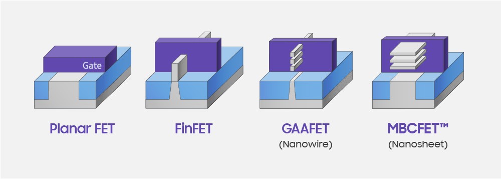
Samsung Foundry has announced that it is beginning to mass-produce its first-generation chips on the 3nm node. It is based on the new GAA (Gate-All-Around) transistor architecture, the next step after FinFET.
Compared to 5nm, Samsung’s first generation 3nm chips can deliver up to 23% better performance, up to 45% less power consumption and 16% smaller footprint.
Samsung’s second-generation 3nm node will be even more impressive – compared to 5nm, Samsung says it will achieve a 50% reduction in power consumption, up to 30% improvement in performance and a 35% reduction in area.

Samsung is now ahead of TSMC, which is expected to begin mass production of 3nm chips in the second half of the year.
Gate-All-Around (GAA) transistor design allows the foundry to downsize transistors without compromising their ability to carry current. The GAAFET design used in the 3nm node is the MBCFET flavor shown in the image below.

The evolution of silicon transistors
Source
